Emby / Etch
3D integration and process effects in superconducting qubit devices
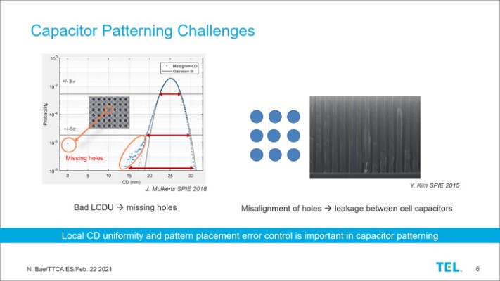
Advanced multiple patterning technologies for high density hexagonal hole arrays
Atomic level control of pattern fidelity during SAC etch
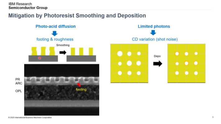
Contact local CD uniformity optimization through etch shrink
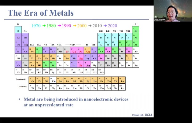
Directional and selective patterning of EUV absorbers
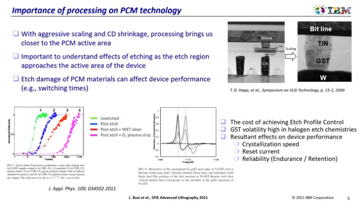
Effect of surface temperature on GeSbTe damage formation during plasma processing
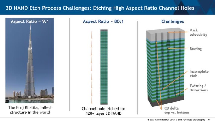
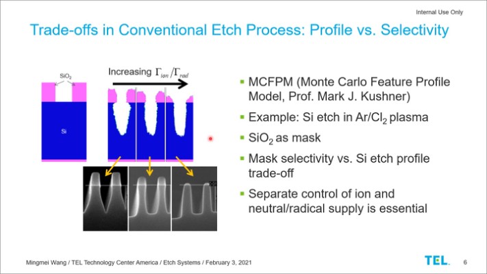
Etch and deposition co-optimization- a pathway to enabling high aspect ratio
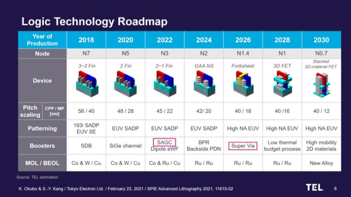
Key challenges and solutions in forthcoming device scaling
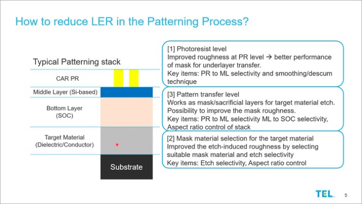
LER reduction strategies for EUV self-aligned double patterning (SADP)
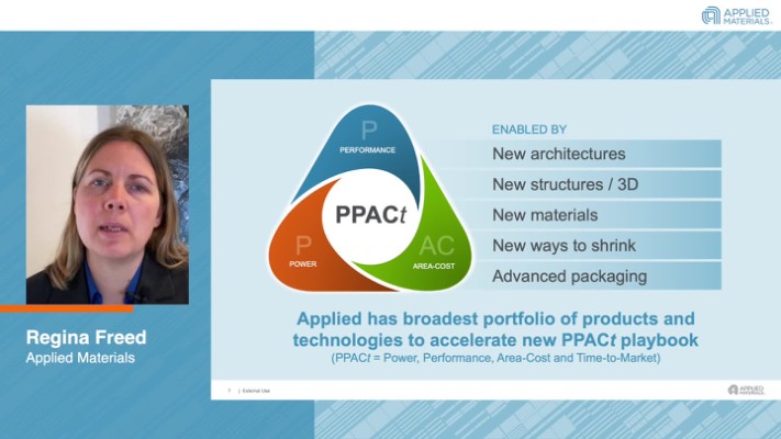
Module-level material engineering for continued DRAM scaling
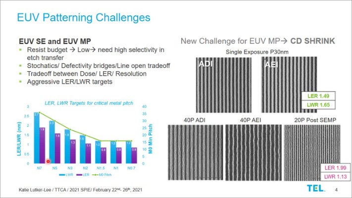
Novel bottom-up organic mandrel growth to enable organic mandrel EUV SADP for sub-5nm node technologies
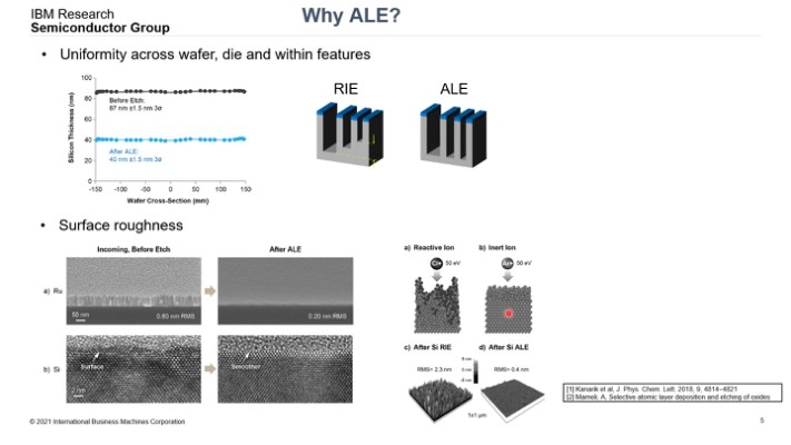
Quasi-atomic layer etching of Si and nitride hard mask with Cl2 based chemistry
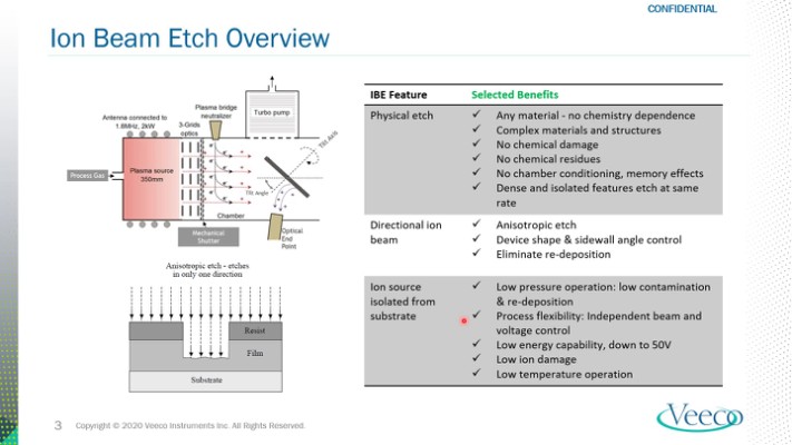
Reactive ion beam etch of slanted gratings for augmented reality_2
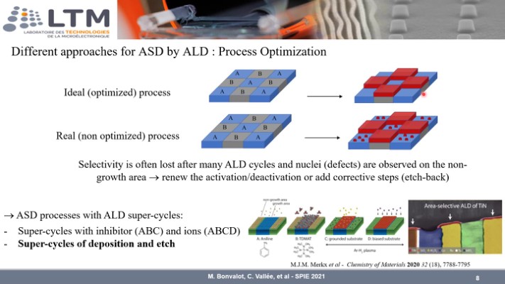
Selective patterning using deposition and etch- case of area selective deposition