Emby / Novel Patterning
Addressing NIL integration for semiconductor device manufacturing
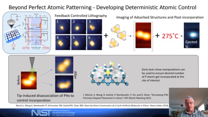
Atomic precision fabrication of quantum devices down to the single atom regime
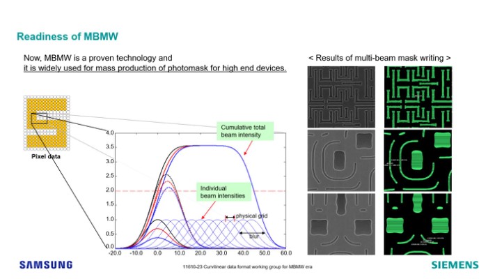
Curvilinear data format working group for MBMW era
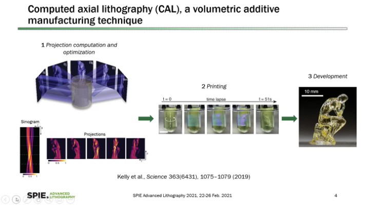
Design of a tomographic projection lithography process for roll-to-roll fabrication of

Design of block copolymers for directed self-assembly
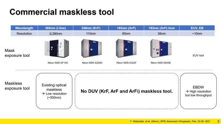
Digital scanner, optical maskless exposure tool with DUV solid state laser
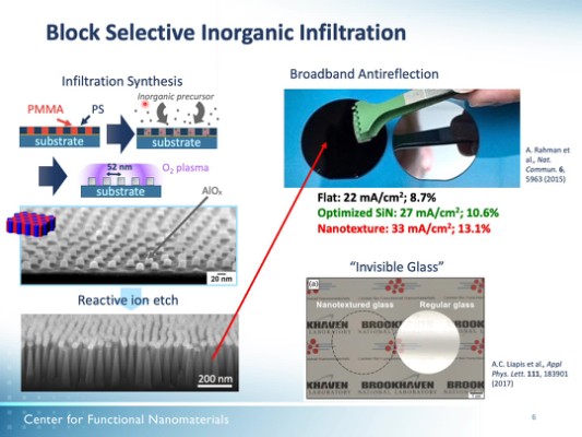
Diversifying the patterning landscape in block copolymer self-assembly
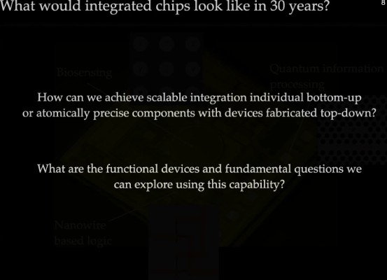
DNA origami- the bridge from top to bottom
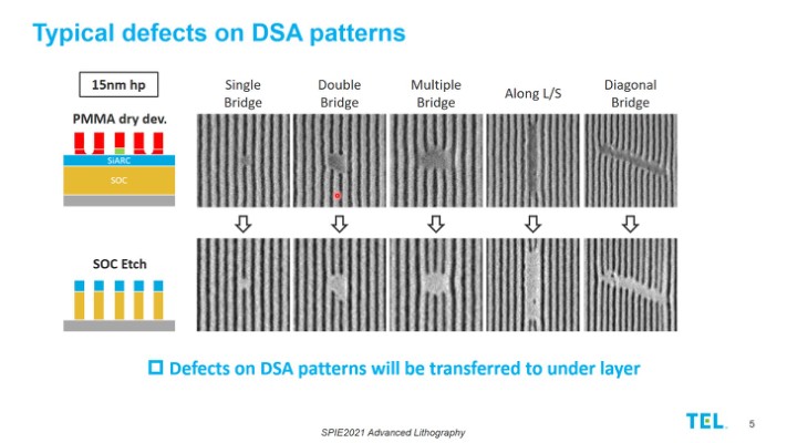
DSA process optimization for high volume manufacturing
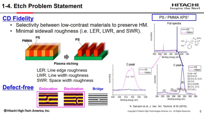
Etch developments in response to DSA challenges
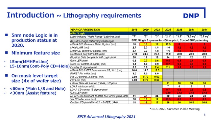
EUV mask process development using MBMW
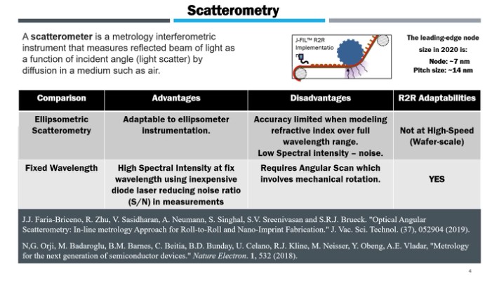
High-speed in-line optical angular scatterometer for high-throughput roll-to-roll nanofabrication
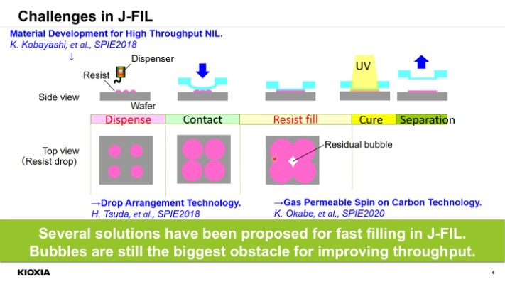
Improvement of productivity by spin coating nanoimprint lithography
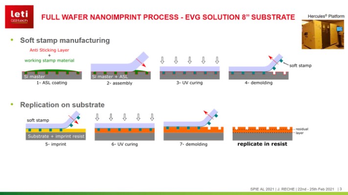
Integration of sub 50 nm features based on EVG SmartNIL for 8-inch substrates
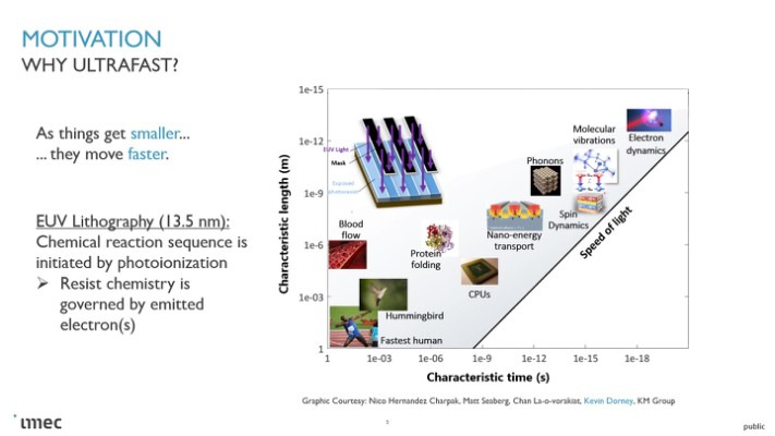
Introduction to imec's AttoLab for ultrafast kinetics of EUV exposure processes and ultra-small pitch lithography
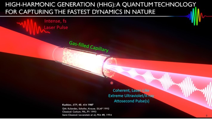
Lloyd’s mirror interference lithography below a 22-nm pitch with an accessible, tabletop, 13.5 nm high-harmonic EUV source
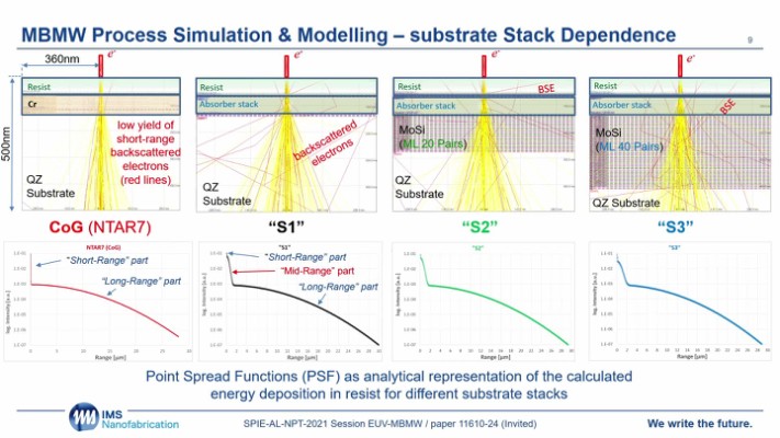
MBMW exposure optimization for EUV mask stacks
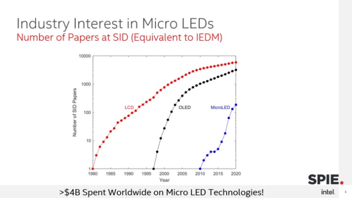
Micro LED displays- technology and manufacturing challenges
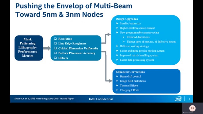
Multi-beam mask writer in EUV era- challenges and opportunities
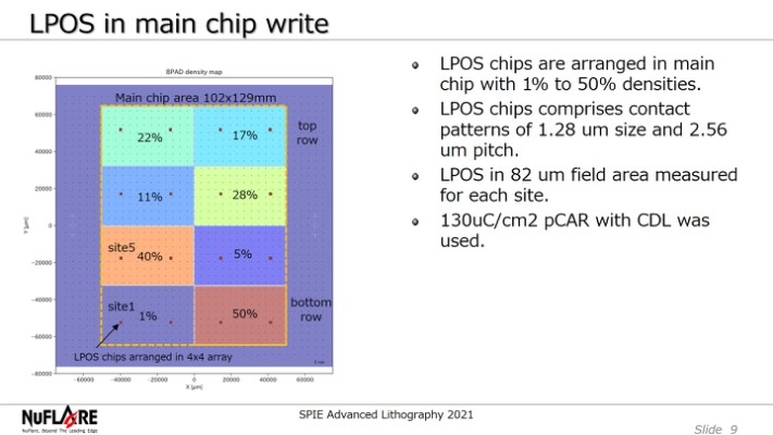
Multi-beam mask writer MBM
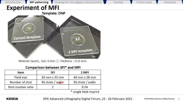
Multi-field imprint technology- enabling the productivity enhancement of NIL
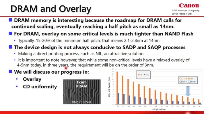
Nanoimprint performance improvements for high volume semiconductor device manufacturing
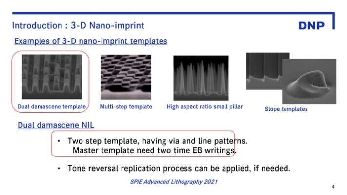
Nanoimprint template development by new fabrication method and its application
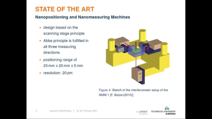
Nanopositioning and -fabrication using the Nano Fabrication Machine with a positioning range up to Ø 100 mm
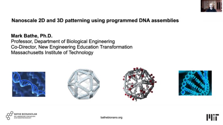
Nanoscale 2D and

A new generation cost-efficient laser mask writer for mature semiconductor nodes

A novel method for generating linear structured illumination using phase modulation